

Samsung Electronics (005930.KS) is strengthening its built-in competitiveness by independently growing devoted software program, because it leads the high-bandwidth reminiscence (HBM) market by vertical integration of reminiscence and foundry (contract manufacturing) operations spanning design to manufacturing. The technique is seen as a transfer to grab the initiative in “customized HBM,” which is poised to grow to be a core part of synthetic intelligence (AI) semiconductors.
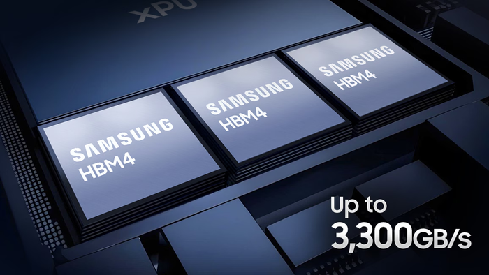
In line with business sources on Wednesday, Samsung Electronics’ success in changing into the primary within the business to ship certified merchandise of the top-performing sixth-generation HBM (HBM4) was backed by the in-house growth of its proprietary “Software program Growth Equipment (SDK).” The SDK, a device that applications HBM alerts whereas verifying defects, is cited as a key issue that accelerated HBM4 growth. Prospects may use the SDK to construct reminiscence architectures that optimize the logic operations of AI semiconductors, establishing it as a gross sales driver as properly.
The SDK converts laptop directions into microcode based mostly on the 0s and 1s that semiconductors can perceive, and injects this into the bottom die (the underside layer) of HBM4. By means of this course of, the bottom die can autonomously right inner errors or tangled alerts throughout knowledge transfers. By means of fifth-generation HBM (HBM3E), the bottom die had a hard and fast circuit construction, so defects might solely be filtered out utilizing designated inspection gear. From HBM4 onward, nevertheless, the bottom die has been modified to a logic (computational) circuit, enabling self-diagnosis by coding.
Behind Samsung Electronics’ institution of its proprietary SDK lies its “vertical integration” construction as an built-in semiconductor firm. Not like opponents that depend on exterior foundries similar to TSMC for base die manufacturing, Samsung Electronics produces not solely the core die (reminiscence layer) based mostly on its reminiscence course of but additionally manufactures the bottom die straight by its foundry course of. It has successfully constructed a “one-stop” system that handles your complete course of underneath one roof. Inside this construction, internalizing the SDK is seen as inevitable for additional accelerating growth pace.
Customized HBM Market Opens… Concentrating on Huge Tech Lock-in through SDK
Because the customized HBM market begins to open in earnest, the SDK is anticipated to grow to be a core gross sales technique for Samsung Electronics. Hyperscalers (operators of ultra-large knowledge facilities) similar to Google, Amazon, and Microsoft are main a wave of adoption of “customized accelerators (ASICs)” optimized for their very own AI computing infrastructure. As a result of every ASIC has completely different logic operations, personalized base die designs are additionally increasing, and the business refers to this as customized HBM.
With general-purpose HBM, there’s inadequate bodily house round AI semiconductors, creating limitations in inserting reminiscence alongside the periphery (shoreline). For purchasers, a brand new breakthrough to resolve knowledge processing bottlenecks is urgently wanted. To handle this problem, Samsung Electronics is remodeling the HBM base die right into a form of controller. This implies it can play the position of straight exchanging knowledge alerts with different exterior reminiscence or community gadgets.
If customized HBM thus establishes itself as a communications hub inside AI semiconductors, even a small error might grow to be a variable that determines general efficiency. Because of this, the significance of Samsung Electronics’ proprietary SDK, which diagnoses sign errors in actual time, is anticipated to develop additional. In the end, if large tech clients construct reminiscence techniques optimized for their very own chips based mostly on the Samsung Electronics SDK ecosystem, a “lock-in” impact will come up, making it troublesome for them to simply change to a different foundry.
“Samsung Electronics is making full-fledged strikes to preempt the market, together with increasing its customized HBM design workforce from the present degree of round 50 folks to 300 this 12 months,” an business official mentioned. “That is proof that world semiconductor firms are giving Samsung Electronics precedence consideration as a customized HBM provide companion.”