Information Abstract:
- NVIDIA CUDA-X libraries and AI fashions are accelerating TSMC workloads throughout lithography, transistor and course of simulation, superior course of management and fab operations optimization.
- TSMC is utilizing NVIDIA Metropolis and NVIDIA TAO Toolkit to advance automated defect inspection with imaginative and prescient AI, enhancing detection of nanometer-scale defects whereas decreasing repeated labeling and retraining.
NVIDIA GTC Taipei—NVIDIA right this moment introduced that TSMC, the world’s main semiconductor firm, is utilizing NVIDIA accelerated computing and AI to advance semiconductor design and manufacturing.
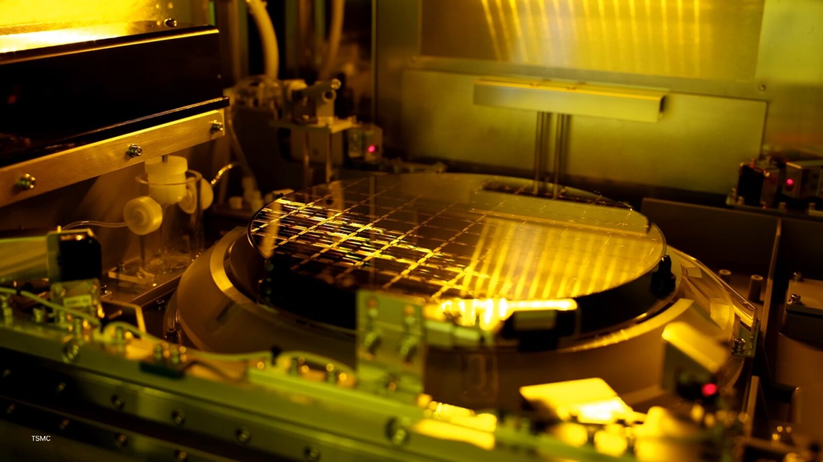
As chips transfer to extra superior nodes, bringing them from design to high-volume manufacturing has grow to be one of many world’s most advanced computing challenges. Computational lithography, transistor simulation, course of management and wafer inspection now require massive-scale simulation and real-time optimization, and AI methods that may present assist throughout physics, photos and different purposes.
TSMC is utilizing NVIDIA applied sciences to speed up this transformation, making use of accelerated computing and AI throughout the semiconductor design and manufacturing lifecycle to enhance turnaround time, vitality effectivity, yield and operational productiveness in superior fabs.
“NVIDIA and TSMC have labored collectively for practically three a long time to push the boundaries of computing,” mentioned Jensen Huang, founder and CEO of NVIDIA. “TSMC is bringing NVIDIA AI and accelerated computing into the fab itself, tackling a number of the world’s most advanced design and manufacturing challenges with simulation, optimization and AI to enhance pace, effectivity and yield for the following era of chips.”
“TSMC and NVIDIA have constructed a long-standing partnership rooted in advancing the applied sciences that make the following era of computing potential,” mentioned C.C. Wei, chairman and CEO of TSMC. “Through the use of NVIDIA accelerated computing and AI throughout fab operations optimization, lithography, course of management and inspection, TSMC is strengthening our know-how management and manufacturing excellence to assist our prospects’ future merchandise and success.”
TSMC Accelerates Processes With NVIDIA CUDA-X Libraries and AI
Superior semiconductor design and manufacturing require huge computational workloads and extremely coordinated fab operations, spanning chip-design switch, transistor modeling, course of management and fab productiveness.
TSMC is utilizing NVIDIA CUDA-X™ libraries and AI fashions to speed up these workloads on NVIDIA GPUs:
- Computational lithography: TSMC is utilizing NVIDIA cuLitho, a GPU-accelerated library for lithography — a printing methodology for chip masks design. This know-how delivers a 20-50% enchancment in price effectiveness or cycle time in contrast with CPU-based computational lithography, whereas sustaining the identical price of possession.
- Transistor, gear and course of simulation: TSMC is utilizing NVIDIA cuEST, a GPU-accelerated digital construction simulation library for 50x sooner chemistry simulations, on common, for semiconductor materials design.
- Superior course of management: TSMC is utilizing the NVIDIA cuML machine studying library to speed up large-scale analytics on NVIDIA GPUs. This lets TSMC pace algorithms and distill tons of of hundreds of course of parameters spanning hundreds of steps as precision inputs for machine studying fashions — making vital discount in course of variation.
- Fab operations optimization: GPU-accelerated scheduling computation utilizing CUDA has led to notable enhancements in fab productiveness with NVIDIA H200 GPUs. By harnessing CUDA-powered computation on NVIDIA H200 GPUs, TSMC has enhanced its functionality to handle advanced constraints, thereby streamlining manufacturing paths and maximizing fab productiveness.
TSMC Advances Defect Inspection With NVIDIA Metropolis and AI Fashions
As chips grow to be extra superior, even the smallest defects can have an effect on high quality and yield, making sooner and extra correct inspection important to semiconductor design and manufacturing.
TSMC is utilizing the NVIDIA Metropolis platform and NVIDIA TAO Toolkit to enhance superior defect classification. Utilizing imaginative and prescient AI, TSMC has improved detection of defects at nanometer scale.
These capabilities assist TSMC enhance high quality inspection whereas decreasing the necessity for repeated labeling and retraining as course of situations, inspection instruments and defect varieties change.
TSMC Faucets NVIDIA Omniverse to Construct FabTwin
Superior semiconductor fabs are among the many most advanced fabs ever constructed, requiring exact coordination throughout instruments, supplies, robots, people and facility methods.
TSMC is exploring NVIDIA Omniverse™ libraries to construct FabTwin, a digital fab setting for evaluating course of device layouts and associated simulation workflows. By testing design eventualities digitally earlier than bodily implementation, TSMC can evaluate advanced configurations extra flexibly and establish potential constraints earlier. This virtual-first method vastly improves planning effectivity and accelerates vital decision-making earlier than any bodily or capital commitments are made.
Watch Huang’s keynote and study extra at NVIDIA GTC Taipei.