
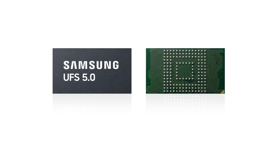
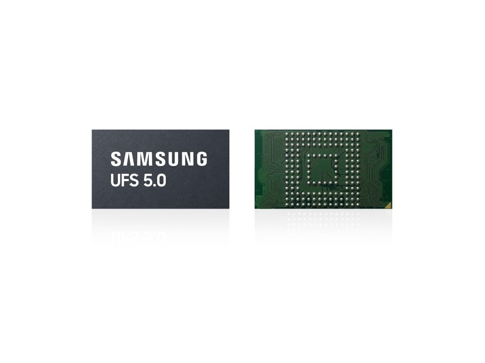
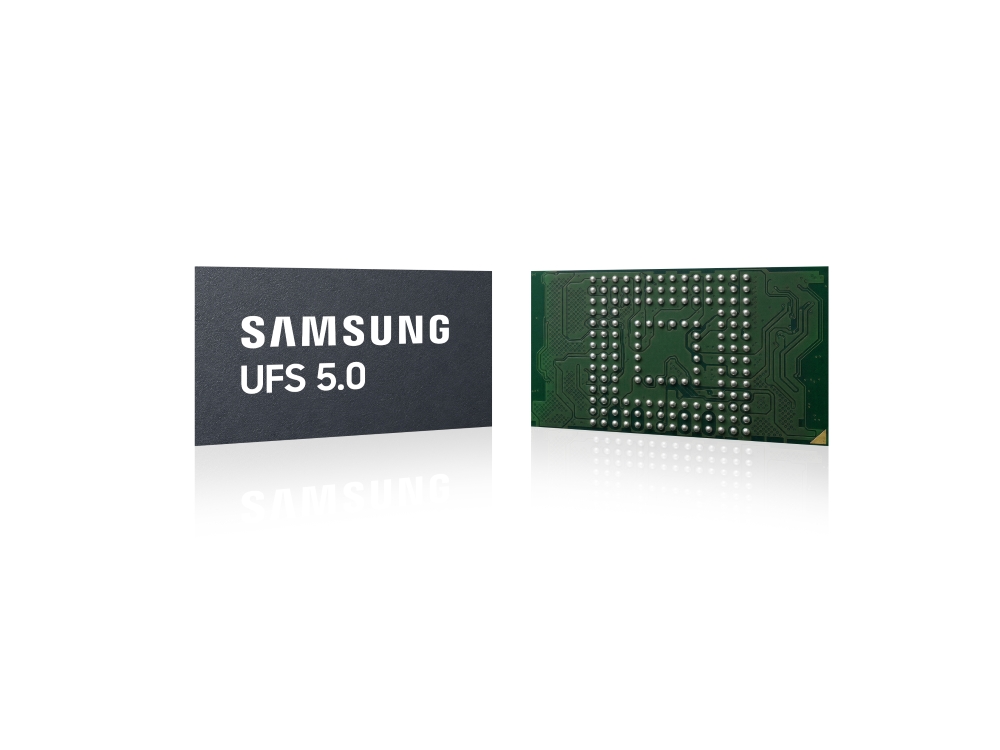
Samsung Electronics, the world chief in superior reminiscence expertise right this moment introduced that, for the primary time within the business, it has developed the business’s quickest Common Flash Storage (UFS) 5.0 answer, which can assist allow seamless and extremely environment friendly AI companies on future cell units.
The milestone units a brand new benchmark for the next-generation cell reminiscence market as the improved efficiency is predicted to permit cell gadget customers with considerably lowered latency and sooner response occasions when operating giant language fashions (LLMs) in on-device AI environments.
“Within the period of on-device AI, storage units are evolving right into a key driver defining AI experiences,” stated Jangseok Choi, head of Reminiscence Product Planning at Samsung Electronics. “As we efficiently transfer past the event stage of the business’s first UFS 5.0 answer, Samsung is setting a brand new customary for storage on the go and can proceed to drive innovation for the next-generation cell platform market.”
Generative AI is quickly shifting from the cloud to the gadget, driving a surge within the scale of information required for native processing. Consequently, storage is evolving from a medium used primarily to retailer information to core infrastructure that helps AI computation.
Samsung’s UFS 5.0 integrates the most recent embedded reminiscence interface customary from JEDEC, attaining unparalleled efficiency ranges with the business’s highest bandwidth of as much as 10.8 gigabytes per second (GB/s).
The brand new storage answer delivers a sequential learn velocity of as much as 10.8 GB/s and a sequential write velocity of as much as 9.5 GB/s, speeds which can be respectively greater than twice as quick as these of the earlier UFS 4.1 customary. This vital development permits a lot sooner storage and processing of enormous information for on-device AI purposes.
Energy effectivity in Samsung’s UFS 5.0 can also be improved by greater than 40% in comparison with the corporate’s UFS 4.1 answer. That is achieved by implementing numerous new improvements, together with clock gating and multi-voltage applied sciences. These enhancements assist to significantly scale back the facility required to switch the identical quantity of information, drastically decreasing total energy consumption and increasing the battery lifetime of next-generation cell units.
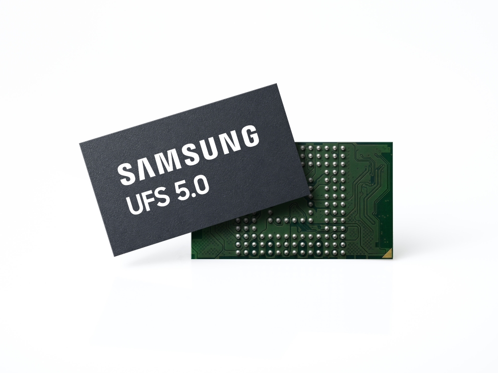
Samsung has engineered the UFS 5.0 answer into an ultra-compact bundle measuring simply 7.5mm x 13mm x 0.9mm — making it 16.7% smaller than its predecessor. This way issue considerably boosts design flexibility and inner house utilization for a variety of purposes, together with cell, wearable and prolonged actuality (XR) units.
Samsung will start mass manufacturing of its UFS 5.0 within the fourth quarter of this 12 months in a wide range of capacities as much as one terabyte (TB). Via this breakthrough in UFS 5.0 expertise, Samsung is staying forward of business wants and plans to scale up provide to fulfill the expansion of next-generation gadget markets — starting from flagship smartphones to XR headsets and AI wearables.